I am a gadget junkie. Anytime a new tech toy hits the market, I’m the first in line to buy one. However, when I bought a digital camera two years ago, it was not the camera itself that held my fascination, it was the cool little matchbook-sized card that stored all the pictures (see Photo 1). As more products appeared that used a CompactFlash card for removable storage, I was both delighted and despondent. Delighted because this seemed to end the apparent curse that my enthusiasm for a new format indicated its obsolescence (i.e., MiniDisc, CDi, etc.). And, despondent because every device that used a CF card seemed to have some serious processing horsepower, making it appear that using such an interface in lower-end designs would be difficult. When I discovered the Microchip PIC microcontroller, I knew it was my solution for integrating CompactFlash into my own projects. Now, I have the capability to add numerous megabytes of compact, removable, nonvolatile memory to virtually any system.
The CompactFlash Association was established in 1995 to specify the format of what was to become a subset of the PCMCIA or PC card specification. The result is a removable media standard that uses fewer interface signals (50 instead of 68) and is roughly one-third the size of a PCMCIA memory card. The internals of the memory card consist of a smart controller, buffer, and varying amounts of nonvolatile memory. The specification also defines different modes of access to the card, including Common Memory mode and True IDE mode. While in True IDE mode, the card can be directly connected to an IDE bus with no active circuitry, which makes it a great way to add removable storage to an embedded PC. However, because I was planning to use an 8-bit microcontroller, I chose to access the CompactFlash card in its Common Memory mode, taking advantage of an 8-bit wide data bus in this mode, instead of the 16-bit data bus required for an IDE interface.
As for the microcontroller, I chose a PIC16F877, one of Microchip’s newer parts. The “F” stands for flash memory, which makes development nicer than the old burn, test, and wait-for-half-an-hourunder-a-UV-light cycle. In addition, Microchip’s integrated development environment (MPLAB) is available (free) from its web site, and an inexpensive in-circuit debugger is available for these flash memory parts.
The basics of the PIC are the same as they are for any other part in the PIC16xxx family, including a RISC design with 35 instructions and a plethora of peripherals. Although this project does not use any of the peripherals built into the device, the main reason for me picking this particular part was that those peripherals are still available for some other use. I had to keep in mind that this is not an isolated project but something that will be integrated into other projects. That is the reason I chose a 40-pin device that has 33 I/O pins when I am only using 17, and could therefore fit into a 28-pin device. In addition, this device has 8 KB of program memory available, yet I am using far less than that. All of these considerations were made with the knowledge that the PIC would be running more than the read and write routines and would be connected to more than just the CompactFlash card.
The theory of operation in interfacing to the CompactFlash card in its Common Memory mode is similar to an IDE interface. In a nutshell, eight registers are accessible by the host and loaded with various data. After the first seven registers are loaded with the appropriate information, the eighth (command) register is loaded with a command, and that command is executed.
To accomplish this, I have a 17-pin connection from the PIC to the card, including three address lines (E2:E0), eight data lines (D07-D00), and six control lines. For an absolute minimum interface to a CF card, a few of these control signals are not necessary. According to the CompactFlash specification, signals CD2 and CD1 are grounded internally to the card to indicate that a card has been inserted. [1] I connect the PIC to CD1 (with a 10-kilohm pull-up), and if the pin is low, a card is present. Another connection that can be removed from the interface is the RDY/–BSY signal. In my example code, I poll this line prior to read and write operations to ensure that the card can accept a command, but a fixed-time delay can also be used if free I/O pins are getting tight.
A third signal that is not absolutely necessary but nice to have is a reset line. Strobing the reset line low will, as the name suggests, reset the controller in the CF card. The other three control lines that I use are CE1, which will connect the card data bus (useful if sharing an 8-bit data bus), the active low OE (output enable), and WE (write enable) strobe signals.
As you can see in Figure 1, the remaining interface lines are fairly straightforward. The three address lines to the card are on Port E, which is conveniently a 3-bit wide port. The eight data lines from the card are connected to Port D, and the control lines are on Port C. So much for the hardware interface.
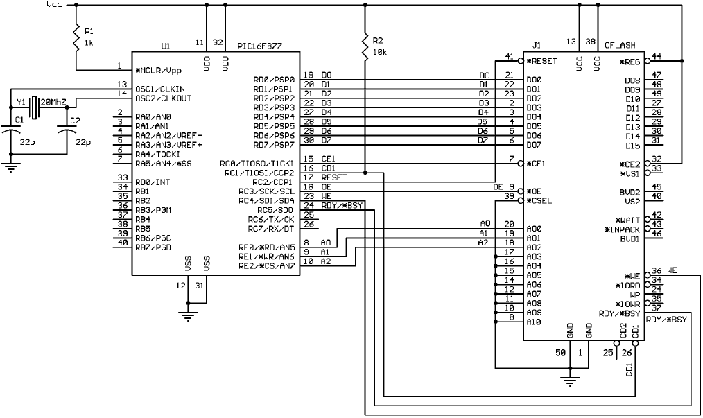
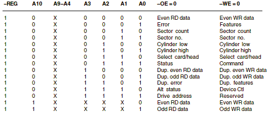
The functional procedure to access the CF card is also easy, after the 116- page CompactFlash Association Specification is dissected. The most important bit of information in the specification is the address decoding of the eight control registers within the controller portion of the card (see Table 1). Access to the full range of necessary registers can be achieved using only three address lines, so –REG and A10–A3 are hardwired to VCC and GND, respectively.
To load one of these registers, the data sent is placed on the data lines to the card, the 3-bit address of the desired register is placed on the address lines, and –WE is strobed low. It’s that easy. By loading the various registers with sector addresses (either in logical block addressing or cylinder/head/ sector addressing) and a command in the command register, commands can be sent to perform a read, write, or any number of other operations. The results of these operations most often go through the internal buffer, and sequential accesses to the data register incrementally access each byte.
For example, if a card has a sector size of 512 bytes, a buffer size of 512 bytes, and the appropriate addressing registers have been loaded followed by a read sector command, the buffer is then loaded with the contents of that sector. The first access to the data register (accomplished by putting the address of the data register on the address bus and strobing –OE) will read the first byte in the buffer. The next strobe of –OE will read the next byte in the buffer and so on.
The same would be true of a write sector operation. After the sector location has been loaded into the appropriate registers and the write sector command has been loaded into the command register, the first byte to be written is placed on the data bus. When –WE is strobed, that byte is written to the first location in the buffer. The next byte to be written is then placed on the data bus, –WE is strobed again, and so on. Because these operations go through the buffer, which is internally read from and written to a full sector at a time even if the desire is only to write one byte to the card, a full 512 bytes must be written to the buffer. The data in the buffer does not transfer to the card memory until the buffer is full.
Almost all CompactFlash cards on the market today have both sector and buffer sizes of 512 bytes. To ensure that’s true for a particular card, use the identify drive command, which can be sent to the card without loading any of the other registers. When the value 0xEC (identify drive) is strobed into the command register, the buffer is immediately filled with 512 bytes of useful information, including sector size, buffer size, model numbers, serial numbers, number of heads, cylinders, tracks, and too many other goodies to be listed here. However, they are well documented in the CompactFlash Association Specification.
The sample source code I have provided for downloading shows a simple application of reading from and writing to a CompactFlash card. The program essentially uses two bytes on a card to store a counter, which keeps track of how many times the card has been inserted into the socket. This is accomplished by waiting for the card detect signal (CD1) to go low, indicating that a card is present.
An identify drive command is executed to get the sector size (word 5) and buffer size (word 21) of the particular card that has been inserted. The identify drive command doesn’t require any parameters, so none of the other registers have to be loaded with any data. Simply load the command register and strobe –WE.
The CompactFlash Association Specification states details about each command and the results, including the breakdown of the 512 bytes of information dispensed by this particular command. To get to a specific piece of information, simply strobe –OE enough times to get to that data in the sequence. For example, the number of bytes per sector is stored in the sixth word (word 5), so strobing –OE eleven times will make the first byte of that particular data field appear on the data bus.
Most of the information on the card is stored as 16 bits, so the subroutine in the code (CF_READ) actually strobes –OE twice, storing the first byte read in DATA_LO and the second byte read in DATA_HI. The program then uses these values to know how many times to write to the buffer before that information is actually transferred from the buffer to the card memory. Next, the program reads a sector at a particular location but only reads the first two bytes from the buffer. These two bytes are the counter, which is incremented and written back to that same location on the card.
One note of caution, running this program on a CF card that has been formatted and has data already stored on it may corrupt that data and make the card unreadable until it is reformatted, because this program will overwrite a specific sector on the card. That read and written location is clearly annotated in the source code, so feel free to play around with the target location and amount of data read or written.
There is a useful shareware application that I used to read the raw hex data from the card to verify the actions of the PIC. The program is called WinHex and is available from CNET and various other shareware archives on the Internet. As long as you have the means to access a CompactFlash card as some sort of disk on your PC, you can use WinHex to view each individual byte stored on the card.
In order to make my development as easy as possible, I took the PIC-to- CF
interface shown in Figure 1, added an IDE connector so I could plug the card
right onto the IDE bus of my PC, added in a full set of test points for each
signal on the CF card (along with in-circuit serial programming and incircuit
debugger headers for the PIC), and had some boards made. The end result was
a nice little development kit. {ed: Available for $99
from:
http://www.armanet.com/Pages/engineeringright.html
}
This simple example program is the backbone of the lowest level of interface to the CompactFlash card. I want to stress that this is only the bare minimum for an extremely simple interface. Additional layers of firmware would be needed to read and store information that spans several sectors, and external memory may be required if the application is not one that caters to streaming data.
This foundation, combined with some deep reading of Microsoft’s FAT specification [2], has allowed me to use a PIC to extract information stored in specific files on a Windows-formatted CF card. Again, there is a lot more overhead that has to go in the PIC program to read various data from the file structure system just to find the location of the file on the card and be able to follow the data through various sectors. However, the actual data on the card is the same, with no regard to the mode of operation of the card (IDE or common memory), so it’s only a matter of understanding any other file specification to be able to conform to that specification within the PIC. Being able to access information on a card that has been formatted to a specific file system is a nice feature, allowing you to simply copy a certain file from a PC onto a CF card. And, the PIC can access the information in that same format, without having to restructure the data into some proprietary configuration.
Being the gadget junkie that I am, it was exciting just being able to read and write a little 2-byte counter on a cool little device. But, using those same basic subroutines, the possibilities are endless. Want to store a year’s worth of a regularly sampled analog signal? Put a PIC and a CompactFlash card on it. Want a digital picture frame? Store bitmap files on a CF card and hook the PIC to an LCD. Want an MP3 player? Keep the music on a CF card and tie the PIC to one of the now readily available MP3 decoder parts.
The point is that CompactFlash cards are a great medium for removable memory, and the format is not going away any time soon. I doubt IBM would have chosen the CompactFlash form factor for its amazing 1-GB Microdrive if support for CF was not going to be around for years to come. And yes, the Microdrive conforms to the CompactFlash card specification, so anything you do to interface to a CF card will also work with the Microdrive (but with a higher current demand). One gigabyte of removable storage for any project you can think of! I love gadgets!
Mark Samuels works at ARMA Design, a custom design house in San Diego, CA, where he does firmware and hardware design for a wide variety of embedded projects, most often using PIC microcontrollers. He can be reached at mark@ARMAnet.com or visit ARMA’s web site at www.ARMAnet.com.
 title  "CompactFlash"
;
;
;
;
  LIST P=16F877, R=DEC
  errorlevel 0,-305,-302
  INCLUDE "c:\progra~1\mplab\P16F877.inc"

;******************************************************************************
;******************************************************************************
;**                                                                          **
;**  COMPACTFLASH CARD TO PIC INTERFACE                                      **
;**                                                                          **
;**  MARK A. SAMUELS                                                         **
;**                                                                          **
;******************************************************************************
;******************************************************************************


;  Registers

 __CONFIG _CP_OFF & _WDT_OFF & _XT_OSC & _PWRTE_ON & _LVP_OFF


; VARIABLE DECLARATIONS
;******************************************************************************
TEMP_W		EQU	0x20
TEMP_S		EQU	0x21
REGA		EQU	TEMP_S + 1
REGB		EQU	REGA + 1
REGC		EQU	REGB + 1
REGD		EQU	REGC + 1
REGE		EQU	REGD + 1
DATA_HI		EQU	REGE + 1
DATA_LO		EQU	DATA_HI + 1
COUNTER_LO	EQU	DATA_LO + 1
COUNTER_HI	EQU	COUNTER_LO + 1
SECTORS_LO	EQU	COUNTER_HI + 1
SECTORS_HI	EQU	SECTORS_LO + 1
BUFSIZE_LO	EQU	SECTORS_HI + 1
BUFSIZE_HI	EQU	BUFSIZE_LO + 1


; PORT DECLARATIONS
;******************************************************************************
CF_DATA		EQU	PORTD
CF_ADDR		EQU	PORTE
CF_CONTROL	EQU	PORTC


; FLAG DECLARATIONS
;******************************************************************************
	; CF CONTROL
CE1		EQU	0	; CF CONTROL PORT, 0 (LOW = ENABLE, HI = HI-Z)
CD1		EQU	1	; CF CONTROL PORT, 1
RESET		EQU	2	; CF CONTROL PORT, 2
OE		EQU	3	; CF CONTROL PORT, 3
WE		EQU	4	; CF CONTROL PORT, 4
RDY		EQU	5	; CF CONTROL PORT, 5


; CF CARD REGISTER ADDRESSES
;******************************************************************************
;  ADDRESS VALUES, LOW 3 BITS AS FOLLOWS:
;		(X,X,X,X,X,A2,A1,A0)

DATA_REG	EQU	0x00		; ADDRESS OF DATA REGISTER
ERROR_REG	EQU	0x01		; ADDRESS OF ERROR REGISTER
FEATURES_REG	EQU	0x01		; ADDRESS OF FEATURES REGISTER
SEC_CNT_REG	EQU	0x02		; ADDRESS OF SECTOR COUNT REGISTER
SEC_NUM_REG	EQU	0x03		; ADDRESS OF SECTOR NUMBER REGISTER
CYL_LO_REG	EQU	0x04		; ADDRESS OF LOW CYLINDER REGISTER
CYL_HI_REG	EQU	0x05		; ADDRESS OF HIGH CYLINDER REGISTER
HEAD_REG	EQU	0x06		; ADDRESS OF HEAD/DRIVE REGISTER
STATUS_REG	EQU	0x07		; ADDRESS OF STATUS REGISTER
COMMAND_REG	EQU	0x07		; ADDRESS OF COMMAND REGISTER

; COMMAND ASSIGNMENTS
;******************************************************************************
; COMMAND VALUES, 8 BITS

IDENTIFY	EQU	0xEC
WRITE_SEC	EQU	0x30
READ_SEC	EQU	0x20


	PAGE

	org 0
	NOP
	goto PRE_MAIN


	org 4
	  goto Int
;******************************************************************************
;******************************************************************************
;**                                                                          **
;**   INTERRUPT SERVICE ROUTINE                                              **
;**                                                                          **
;******************************************************************************
;******************************************************************************
; (NO INTERRUPTS IN THIS CODE... ONLY HEADER AND FOOTER FOR ISR)

Int
	movwf	TEMP_W
	swapf	STATUS, w
	movwf	TEMP_S

; check int source here


	goto	End_of_Int


End_of_Int

	swapf	TEMP_S, w
	movwf	STATUS

	swapf	TEMP_W, f
	swapf	TEMP_W, w

	retfie

;*****************************************************************************
;*****************************************************************************
PRE_MAIN
;*****************************************************************************
;*****************************************************************************
; CLEAR MEMORY SPACE (SET ALL RAM VALUES TO 0x00)


	BCF	STATUS, RP0
	BCF	STATUS, RP1

	MOVLW	0x20
	MOVWF	FSR

	CALL	CLEAR_MEM

	BSF	STATUS, IRP

	MOVLW	0x20
	MOVWF	FSR

	CALL	CLEAR_MEM

	BCF	STATUS, IRP

	BCF	STATUS, RP0
	BCF	STATUS, RP1

	GOTO	INIT_DONE

CLEAR_MEM
INV_010
	CLRF	INDF
	INCF	FSR, F

	MOVLW	0x80
	SUBWF	FSR,W
	BTFSS	STATUS, Z
	GOTO	INV_010

	MOVLW	0xA0
	MOVWF	FSR

INV_020
	CLRF	INDF
	INCF	FSR, F

	MOVLW	0x01
	SUBWF	FSR,W
	BTFSS	STATUS, Z
	GOTO	INV_020

CLEAR_MEM_END
	RETURN

INIT_DONE

; Setup

	BSF	STATUS, RP0            ;  Goto Bank 1

	MOVLW	0x00

	MOVWF	TRISC		;  Set RC(7:0) as outputs
	MOVWF	TRISD		;  Set RD(7:0) as outputs
	MOVWF	TRISE		;  Set RE(2:0) as outputs

	MOVLW	0xFF
	MOVWF	TRISA		;  Set RA(5:0) as inputs
	MOVWF	TRISB		;  Set RB(7:0) as inputs


	BSF	CF_CONTROL,CD1	; MAKE CD1 AN INPUT (CARD DETECT)
	BSF	CF_CONTROL,RDY	; MAKE RDY AN INPUT (RDY/BSY)

	MOVLW	0x06			;  Set PORTA as digital I/O
	MOVWF	ADCON1

	MOVLW	0xA0			;
	MOVWF	OPTION_REG

	BCF	STATUS, RP0            ;  Go back to Bank 0
	MOVLW	0x00
	MOVWF	ADCON0

;**********************************************************************
;**********************************************************************
MAIN
;**********************************************************************
;**********************************************************************
	MOVLW	0x18
	MOVWF	CF_CONTROL

	MOVLW	0x00
	MOVWF	CF_ADDR


CHK_CARD
	BTFSC	CF_CONTROL, CD1		; CARD INSERTED?
	GOTO	CHK_CARD		; NO, GO BACK

					; YES, GO ON

	BSF	CF_CONTROL, RESET	; RESET CF CARD
	NOP
	NOP
	BCF	CF_CONTROL, RESET
	NOP
	NOP

	CALL	HALF_SEC


	; WRITE CF EXECUTE IDENTIFY DRIVE COMMAND (0xEC)

	MOVLW	COMMAND_REG		; REGISTER TO BE ADRESSED
	MOVWF	CF_ADDR

	MOVLW	IDENTIFY		; INSTRUCTION CODE
	MOVWF	CF_DATA

	CALL	CF_WRITE

	; READ DATA REGISTER
	MOVLW	READ_SEC
	MOVWF	CF_ADDR

	MOVLW	.5	; DROP FIRST 5 WORDS
	MOVWF	REGA
TRUNC1
	CALL	CF_READ
	DECFSZ	REGA,F
	GOTO	TRUNC1

	; READ AND STORE THE NUMBER OF BYTES PER SECTOR
	CALL	CF_READ
	MOVF	DATA_HI, W
	MOVWF	SECTORS_HI
	MOVF	DATA_LO, W
	MOVWF	SECTORS_LO

	; SUBTRACT 64 FROM NUMBER OF BYTES PER SECTOR (OFFSET)
	MOVLW	0x40
	SUBWF	SECTORS_LO, F		; SUBTRACT FROM LOW BYTE
	BTFSS	STATUS, C		; NEGATIVE RESULT?
	DECF	SECTORS_HI, F		;  YES, SUBTRACT 1 FROM HI BYTE


	MOVLW	.15	; SKIP NEXT 15 WORDS
	MOVWF	REGA
TRUNC2
	CALL	CF_READ
	DECFSZ	REGA,F
	GOTO	TRUNC2

	; READ AND STORE THE BUFFER SIZE

	CALL	CF_READ
	MOVF	DATA_HI, W
	MOVWF	BUFSIZE_HI
	MOVF	DATA_LO, W
	MOVWF	BUFSIZE_LO


	; READ SECTOR 256 (LBA 0x100)
	MOVLW	0xE0
	MOVWF	CF_DATA
	MOVLW	HEAD_REG
	MOVWF	CF_ADDR
	CALL	CF_WRITE

	MOVLW	0x00
	MOVWF	CF_DATA
	MOVLW	CYL_HI_REG
	MOVWF	CF_ADDR
	CALL	CF_WRITE

	MOVLW	0x01
	MOVWF	CF_DATA
	MOVLW	CYL_LO_REG
	MOVWF	CF_ADDR
	CALL	CF_WRITE

	MOVLW	0x00
	MOVWF	CF_DATA
	MOVLW	SEC_NUM_REG
	MOVWF	CF_ADDR
	CALL	CF_WRITE

	MOVLW	0x01
	MOVWF	CF_DATA
	MOVLW	SEC_CNT_REG
	MOVWF	CF_ADDR
	CALL	CF_WRITE

	MOVLW	READ_SEC
	MOVWF	CF_DATA
	MOVLW	COMMAND_REG
	MOVWF	CF_ADDR
	CALL	CF_WRITE


	MOVLW	DATA_REG
	MOVWF	CF_ADDR

	; READ AND STORE COUNTER WORD
	CALL	CF_READ
	MOVF	DATA_HI, W
	MOVWF	COUNTER_HI
	MOVF	DATA_LO, W
	MOVWF	COUNTER_LO

	; INCREMENT COUNTER
	INCF	COUNTER_LO,F
	BTFSC	STATUS,Z
	INCF	COUNTER_HI,F


	; WRITE SECTOR 256 (LBA 0x100)
	MOVLW	0xE0
	MOVWF	CF_DATA
	MOVLW	HEAD_REG
	MOVWF	CF_ADDR
	CALL	CF_WRITE

	MOVLW	0x00
	MOVWF	CF_DATA
	MOVLW	CYL_HI_REG
	MOVWF	CF_ADDR
	CALL	CF_WRITE

	MOVLW	0x01
	MOVWF	CF_DATA
	MOVLW	CYL_LO_REG
	MOVWF	CF_ADDR
	CALL	CF_WRITE

	MOVLW	0x00
	MOVWF	CF_DATA
	MOVLW	SEC_NUM_REG
	MOVWF	CF_ADDR
	CALL	CF_WRITE

	MOVLW	0x01
	MOVWF	CF_DATA
	MOVLW	SEC_CNT_REG
	MOVWF	CF_ADDR
	CALL	CF_WRITE

	MOVLW	WRITE_SEC	; WRITE WITH ERASE
	MOVWF	CF_DATA
	MOVLW	COMMAND_REG
	MOVWF	CF_ADDR
	CALL	CF_WRITE

	MOVLW	DATA_REG
	MOVWF	CF_ADDR


	MOVF	COUNTER_LO,W
	MOVWF	CF_DATA
	CALL	CF_WRITE
	MOVF	COUNTER_HI,W
	MOVWF	CF_DATA
	CALL	CF_WRITE


	; FILL REST OF BUFFER WITH ZEROS

	CLRF	CF_DATA
	MOVF	BUFSIZE_LO, W		; NUMBER OF 512 BYTE BLOCKS IN BUFFER
	MOVWF	REGE
	MOVLW	0xFE			; 256 BYTES, MINUS 2 ALREADY WRITTEN (COUNTER)
	MOVWF	REGC


TO_END_1
	MOVLW	0x02			;---------------------------------------\
	MOVWF	REGD			;                                        |
					;                                        |
TO_END_2				;                                        |
	CALL	CF_WRITE		;-----\-----------------\                |
	DECFSZ	REGC, F			;      |- 256 TIMES      |               |
	GOTO	TO_END_2		;-----/                  |_ LOOP TWICE   |
					;                        |               |- "BUFSIZE_LO" TIMES
	DECFSZ	REGD, F			;                        |               |
	GOTO	TO_END_2		;-----------------------/                |
					;                                        |
	DECFSZ	REGE, F			;                                        |
	GOTO	TO_END_1		;----------------------------------------/


; LOOP FOREVER UNTIL CARD REMOVED, THEN RESET

END_CHK
	BTFSC	CF_CONTROL,CD1
	GOTO	CHK_CARD
	GOTO	END_CHK

; END OF MAIN LOOP


;******************************************************************************
;*  CHECK_READY SUBROUTINE                                                    *
;******************************************************************************
CHECK_READY
	; CHECK IF CF READY

	BTFSS	CF_CONTROL,RDY
	GOTO	CHECK_READY

	NOP
	RETURN
;******************************************************************************
;*  CF WRITE SUBROUTINE                                                       *
;******************************************************************************
CF_WRITE

	; ENSURE CARD IS READY

	CALL	CHECK_READY
	NOP

	; STROBE "WE" LINE LOW

	BCF	CF_CONTROL, WE
	NOP
	NOP
	NOP
	BSF	CF_CONTROL, WE
	NOP

	RETURN

;******************************************************************************
;*  CF READ SUBROUTINE                                                        *
;******************************************************************************
CF_READ
	; READ TWO BYTES

	CALL	CHECK_READY

	; SET TRIS REGISTERS FOR DATA LINES TO INPUT

	BSF	STATUS, RP0
	MOVLW	0xFF
	MOVWF	CF_DATA
	BCF	STATUS, RP0
	NOP
	CLRF	CF_DATA

	; SET OE LINE LOW
	NOP
	BCF	CF_CONTROL, OE
	NOP
	NOP
	NOP

	; READ AND STORE BYTE #1
	MOVF	CF_DATA,W
	MOVWF	DATA_LO
	NOP
	; SET OE LINE HI
	BSF	CF_CONTROL, OE
	NOP
	NOP

	CALL	CHECK_READY

	; BYTE #2

	; SET OE LINE LOW
	NOP
	BCF	CF_CONTROL, OE
	NOP
	NOP
	NOP

	;READ AND STORE BYTE #2
	MOVF	CF_DATA,W
	MOVWF	DATA_HI
	NOP
	; SET OE LINE HI
	BSF	CF_CONTROL, OE
	NOP

	; CHANGE CF_DATA BACK TO OUTPUT

	BSF	STATUS, RP0
	CLRF	CF_DATA
	BCF	STATUS, RP0
	NOP

	RETURN

;************************************************************************
;*  ONE_SEC                                                             *
;*    GENERATES ONE SECOND DELAY                                        *
;************************************************************************
ONE_SEC
	MOVLW	.255
	MOVWF	REGD
	GOTO	ONE100

HALF_SEC
	MOVLW	.128
	MOVWF	REGD

ONE100
	CALL	DELAY

	DECFSZ	REGD,F
	GOTO	ONE100

	RETURN

;******************************************************************************
;*  DELAY SUBROUTINE                                                          *
;******************************************************************************
DELAY
	MOVLW	.10			; # OF 1MS DELAYS
	MOVWF	REGB

DL100
	CLRF	REGC

DL200					;------\
	NOP				;	\
					;	 \
	DECFSZ	REGC,F			;         > 1 MS (APPROX)
	GOTO	DL200			;	 /
					;	/
	DECFSZ	REGB,F			;------/
	GOTO	DL100			;


	RETURN

;------------------------------------------------------------------------------

	end
| file: /Techref/mem/flash/cf2pic.htm, 25KB, , updated: 2006/4/14 21:41, local time: 2025/10/29 23:26,
216.73.216.50,10-8-63-169:LOG IN
|
| ©2025 These pages are served without commercial sponsorship. (No popup ads, etc...).Bandwidth abuse increases hosting cost forcing sponsorship or shutdown. This server aggressively defends against automated copying for any reason including offline viewing, duplication, etc... Please respect this requirement and DO NOT RIP THIS SITE. Questions? <A HREF="http://massmind.org/Techref/mem/flash/cf2pic.htm"> PIC 2 CF</A> |
| Did you find what you needed? |
Welcome to massmind.org! |
Welcome to massmind.org! |
.