 Tobias
Frost says:
Tobias
Frost says:
Tobias
Frost says:
Tobias
Frost says:
This (private) project has been designed for these purposes:a) Get a Programmer for the ATMEL AVR with USB Interface, as my laptop has no parallel / serial port. As all the ports are on feed through, it is also possible to programm the AVR to get a JTAG interface.
b) Get the possibility to play with several USB IC's: e.g.TUSB 3510 and FTDI 232BM. The TUSB is interesting, but there's no SW available, so as fallback the FTDI can be used)
c) Get a rapid prototyping board for the ATMEL AVR: a "daughter" board can be put on top of the board, and access all the ports of the Atmel.
Also it is possible to generate daughterboards for all the AVR's, so you are not limited to the 8515. With a little effort (JTAG Programming SW) also the new MCUs can be used....
Scalability was a goal, too
Tobias Frost
tobi (at) coldtobi (dot) de
Development Engineer
All Files:

USB Programmer by Tobias Frost
"Copylefted" by Tobias Frost 2005
tobi (at) coldtobi.de
Version: March 30th, 2005
Schematic-Version: 10/03/2005 (DD/MM/YYYY) (CVS 1.6)
This USB Programmer has been entered into the Olimex PCB Pool Contest.
This file describes the hardware, as because of lack of time (and build
hardware) no software is availavle at this time.
The schematic is done with the freeware Eagle Version, available at cadsoft.de.
WARNING: I DO NOT HAVE TESTED THE SCHEMATIC YET. THEREFORE IT CAN BE, THAT IT
WONT WORK OR EVEN DAMAGE SOMETHING (E.G YOUR COMPUTER)! USE AT YOUR OWN RISK!
If you have any remarks or questions, please feel free to contact me.
1. License
USB Programmer Design for the ATMEL AVR MCU
Copyright (C) 2004 Tobias Frost
This project is a free project; you can redistribute it and/or modify
it under the terms of the GNU General Public License as published by
the Free Software Foundation; either version 2 of the License, or
(at your option) any later version.
This project is distributed in the hope that it will be useful,
but WITHOUT ANY WARRANTY; without even the implied warranty of
MERCHANTABILITY or FITNESS FOR A PARTICULAR PURPOSE. See the
GNU General Public License for more details.
You should have received a copy of the GNU General Public License
along with this project; if not, write to the Free Software
Foundation, Inc., 59 Temple Place, Suite 330, Boston, MA02111-1307USA
Additionally to the GPL:
If you are programming for this project
- a TUSB device driver (TUSB firmware or/and PC-Side driver)
- a FDTI bit banging device driver
that you also place this drivers under GPL, and therefore make the source available.
(As I designed the board for free, I think I can expect everyone using this project will
understand, that if you take you can also give.)
If you unable to open your work, please contact me. I am sure that we can find a solution.
Also if you want to commercially resale the board, please contact me.
In other words: Any deviration from the license above needs my written permission.
2. Software
At the moment, there is no software for this project.
But as this project is very generic, this is no limitation for the
usability, as it is designed to work as as "development" board.
But there are plans to programm some kind of firmware, with this support:
- Programming AVRs "incircuit" PC driver/application for the TUSB or
the FTDI ("Bit Banging Mode") would be required to do this. All the
needed pins are routed to the chip (HELP WANTED)
- Programming Software for programming a controller on a daughter
board. First the "old" AVRs are interesting, but also JTAG
programming would be really nice.. The AVR SW should take the data
using the RX/TX Interface of the USB Chips, and the protocol
compatible to the AVR Studio. For these tasks, PC device drivers are
available for the FTDI, (Windows and Linux), so there should be only
need for the AVR SW.
If you like to volunteer to participate in programming, please contact me!
Soon I will put the project's information on my website, so please visit
"www.coldtobi.de/usbprog/", or mail to "usbprog@coldtobi.de" to get informed,
as soon the website gets online.
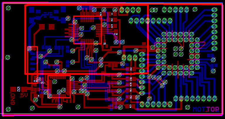
3. Hardware
This is the main part of the docmument: A hopefully not so short description of
the hardware.
Generally, my design uses SMT (Surface mounted technology) heavily. This was
because I like this more than THT (through hole technology) as I hate to drill
a lot....
Also, some of the parts are not available in THT, especially that USB IC's I
use.
But (may with exception of these ICs), I use only "1206" or "0805" SMDs, and
they are easy to handle. All you need is a fine soldering iron, thin solder and
a tweezer.
Let's start with the hardware...
3.1 Power Supply
The design is "Bus powered". The IC1 is a linear voltage regulator, making from
the USB 5V the at some points required 3V3.
Nothing special at this point.
Signals: Description
USB-5V 5V from USB Bus.
3V3 Regulated 3.3 V
GND Ground
Note: There is no reverse voltage protection. This should be not a problem, as
USB is keyed.
Note2: Do _NEVER_ inject power into the USB bus. This can damage your computer.
Note3: Only power small loads from the USB. If using more than 100mA in total,
make sure you are familiar with the USB Specs...
3.2 USB Connector
The connector connects (as the word says) the board from the USB bus to the
transceiver IC's.
I used a SAMTEC Connector, as it was the only one with SMD-pins I was able to
obtain.
Only one transceiver can be used at one time, so I introduced several jumpers
to route the signals. Please solder the jumper in that way, that the signal
"goes" to the right IC.
The signals at the jumper prefixed with "T" go to the TUSB, the "F" ones to the
FTDI. The jumpers' middle pins are connected to the USB Connector, Pin 1 is
connected to the TUSB, Pin 3 to the FTDI.
Signal Jumper Description
D+ SJ7 The "+" Data Signal of the USB
D- SJ8 The "-" Data Signal
3.3 TUSB 3510
The manufactor of this USB Interface is Texas Instruments.
This USB Controller has an 8051 compatible MCU core, and has to be programmed
to be functional. Unfortunaltly, the documentation about the controller
is not very detailed, so I expect some work to compelete the TUSB-side driver.
However, I found on the net an example implementation of a sample driver from
Bodo Rzany. I will add this driver to this package, so please look out for the
file "tusb3410-firmware.tgz".
3.3.1 TUSB support parts
The schematic incorporating the TUSB is mainly taken from the data sheet. So
the suspend schematic is also applied (See datasheet, section Application
Notes)
Also, all pins are accessible, as all are connected to SMD-Pads. If you need
-- as an example -- remote wakeup, it's possible.
Now, a special note on the Diodes D3 to D8: As the TUSB operates on 3.3 V only,
As the AVR can operate on 5V, the inputs have to be protected. This is done
with these diodes, as they should have a zener voltage of 3.3 Volts. The
current is limited by the resitors later toward the AVR. Even if the AVR is
operated on 5V, the 3.3V are sufficient for the AVR to receive a logical
"High".
The crystal's frequency is 12MHz. Please refer to the datasheet for details!
3.3.2 TUSB EEPROM Interface
The TUSB can load it's programm over the bus and using a SPI EEPROM. As I do
not plan to use this feature, but to be open as possible all signals are
accessable: The part "SV8" gives access to SCLK, SDATA, 3.3V and GND. See the
schematic for details.
3.3.3 TUSB Serial Lines
The TUSB has a built in serial port with all the needed support ports. The
signals are prefixed "T" for TUSB and not all used for the AVR connection
described below.
3.3.3 TUSB's DIO
The TUSB has 4 DIOS (Digital Input/Output). In my design, these port are
connected to programm the AVR. Details are in the "AVR Connection" Chapter,
below. The table only shows the connection, if the jumpers are soldered correctly.
TUSB AVR I/O Function
P3_0 MOSI I/O MOSI Pin
P3_1 MISO I/O MISO Pin
P3_3 TRESET I/O Reset Pin (Must be set to "high" in "normal operation")
P3_4 TSCK I/O SCLK Pin
3.4 FTDI 232BM
The FTDI 232BM is a USB-to-serial convertor chip. The manufactor is FTDI
(www.ftdichip.com).
Note: This chip is the second generation of the USB Transeiver!
This chip has no microcontroller included, but should offer the same
functionality as the TUSB built into silicon:
- Serial convertor (USB->RS232)
- "Bit Banging" inteface (Programming the AVR over USB)
For the first feature, there are drivers available. For Windows from the
manufactor, and for linux there's kernel support. (AFAIK a kernel of 2.4.xx or
later is ok)
For the second feature, there MIGHT be some programming effort necessary,
and I heard, that this feature is again not well documentated.
The Jumper SJ10 sets the IO-Voltage of the IC. Please set it to the
appropiate Voltage, probably the AVR Voltage:
SJ10:
3.3V 1-2 closed
5V 2-3 closed
3.4.1 FTDI Support Parts
Also, this chip has needs some parts. For these, I also used the datasheet to
develop it.
The crystal to be used should be 6 MHz. The C7 and C8 crystal loads are in the
area of 27pF.
3.4.2 EEPROM
Also this IC can get its USB Configuration from a external EERPOM. This time,
the EEPROM is a SPI one.
Please read the Datasheet for an example who to connect the EEPROM and what
types are supported.
See the schematic for the EECS, EESK and EEDATA pins. They are connected on the
Board to SMD-Pads,
NOTE:
3.4.3 Serial Connection
The FTDI Serial Cell is connected as described below in the AVR Connection Section.
The control lines are not used in the design. They are prepared to be used in the
"Bit Banging Mode" to programm the AVR.
FTDI-Pin AVR FDTI-Function Description
RTS MOSI OUT MOSI
DTR SCK OUT SCK
DSR MISO IN MISO
DCD RESET IN RESET. Erronous connected. See Errata below!
3.4.4 Bit Banging Interface
To programm the onboard AVR, the Bit Banging Mode can be used. As aleady stated, this needs
software to support this.
However, in the AVR Connection Section, this is detailed.
4. AVR
The AVR 8515 has been put on a socket, and therefore can be replaced. Also it is possible, that
no controller is used. For example, in this case a "daughter board" can be used to connect another
controller,
The AVR has its own crystal and is connected to the USB circuit via the serial interface and/or
the built in SPI Interface, also usable for in-circuit reprogramming.
It is possible to power the AVR with different voltages: 3V3, 5V and external power.
This is determined by SJ9:
5V 1-2 closed (2-3 open)
3V3 2-3 closed (1-2 open)
external Jumper open. External power applied though SV6 and SV7.
Please set
5. Jumpers and AVR Inter-Connection
As already noted, one USB Chip can be used at a time. To get the signals to
the AVR, several jumpers should be set
To connect to the TUSB, the "T"-Prefixed signals has to be routed to the
"AVR"-Prefixed-Signals. This is done with shorting Pins 2 and 3.
To use the FTDI, short pins 1 and 2.
The following table gives a summary about the important jumpers.
Serial:
SJ5 "AVR Rx"
SJ6 "AVR Tx"
SPI programming interface :
SJ1 "AVR Reset"
SJ2 "AVR MOSI"
SJ3 "AVR MISO"
SJ4 "AVR SCK"
USB Input:
SJ7 "USB Data +" (Note: 1-2 is TUSB, 2-3 is FTDI here)
SJ8 "USB Data -" (Note: 1-2 is TUSB, 2-3 is FTDI here)
ERRATA:
Flaws that are found after giving the board to the contest...
1. Flaw:
The FTDI's PWRCTL Pin should not be tied to F3V3 in any circumstances.
According to the datasheet, it should be connected to VCIO
So, if you are using 5V as I/O Voltage, the pin is not connected to the
right voltage.
Fix:
Better would be connecting to VCIO
Best would be a jumper with the options GND and VCIO
Workaround:
- Use 3V3 as IO-Voltage
OR
- Ripup the F3V3 line at pin 14 of the IC, and connect it to pin 13....
Description:
The pin PWCTL determines, if we are self-powered or bus-powered. If the pin is
at VCIO, we are self powered, else we are bus-powered.
If you set VCIO to 5V, the pin is at 3V3,a
2. Flaw:
There should be a serial resistance in the D+ and D- Path, at least for the FTDI
Fix:
Instead of shorting the jumper at D+ and D-, solder in a 22 Ohm resistor
Description:
This was in the FTDI-Datasheet. I think it will work without it, but as the correction
is that easy, it should be done this way....
3. Flaw
The names of the FTDI-EEPROM-Connection-SMD-Pads are wrong. They have been
copied and then forgotten to be renamed. So if you see the pads TXLED1 RXLED1
and TXDEN1 (note the extra "1" at the end of the name), they are for the
EEPROM:
TXLED1 -- EESK
RXLED1 -- EEDATA
TXDEN1 -- EECS
4. Flaw
The FTDI BitBanging Pin for RESET is not usable for this purpose, as this is a input pin.
Workaround:
Connect "TXDEN" to "DCD". Fortunaltly TXDEN has a SMD-Pad and DCD has a via nearby....
(Note: This is only a problem, if someone developes a bit banging device driver....)