This page is for the new versions, Versions 5 or 6, of our break out board. The old version 4 instructions are here: 4axis4build
NEW! Video instructions for building the most common options of the
BOB Panel board:
http://www.youtube.com/playlist?list=PLI15PZTw-OdWB6CF-BK3OXAmdMG2iqnL-
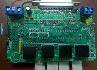
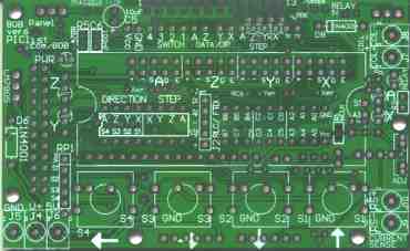
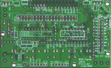
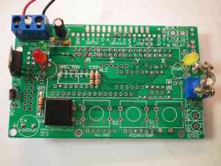
4Axis Break out / Multi-Purpose PCB build instructions: This page documents construction as a break out board for up to 4 THB6064AH, Linistepper, SLAm or other PMinMO^ drivers. There are many options for this board, and not all relate to this use. As a break out board, most users will be interested in the following options:
 |
|
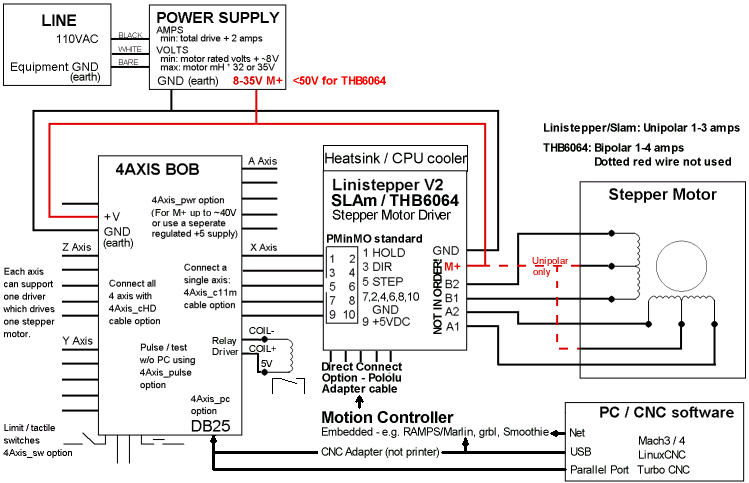 Most people will want to use the
4Axis board to support a stepper motor driver. Click block diagram for
larger version.
Most people will want to use the
4Axis board to support a stepper motor driver. Click block diagram for
larger version.
Click schematic for larger version in a new window.
There is also a google spreadsheet that shows the combination of connections
and helps clarify why they were setup as they were
^
Changes between version 4-5 and version 6 are indicated
in green
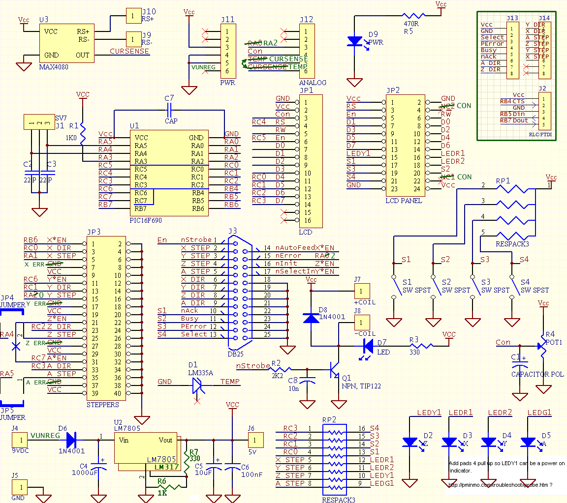
Don't let the schematic scare you! Pretty much the entire top half are items that will probably not be used, but were easy to work into the PCB for future expansion, we can ignore them for now. The only important bits are the power regulator in the bottom left, the STEPPERS header just above it which cables out to 4 stepper drivers (e.g. THB6064AH, Linistepper or SLAm) and the DB25 connector to the right which feeds those drivers from the PC parallel port. The nStrobe signal (see just below and right) drives a relay with LED indicator if you like. RP1, on the right edge, mid way down, pulls up a set of 4 switches which can be installed on the PCB as stop/jog switches or can be wired to limit switches or any other connect to ground switch for feedback to the PC. Combining all these functions on one printed circuit board was more cost effective than making multiple different boards, but you may not wish to populate all the parts of the board; To make different configurations easy, we sell each option as the separate kit of parts:
| Kit |
Parts |
Specs |
QTY |
Description |
 |
||||
| PCB1 | Two Layer, plated through holes, silkscreen, soldermask | 1 | The printed circuit board only: | |
 |
||||
| J3 | DB25, Female, Solder tail | 1 | DB25 pushes on to edge of PCB | |
| CBL | DB25, Male-Male | 1 | Cable to connect to PC Parallel Port | |
 |
||||
| U1 | PIC12F675, DIP 8 | 1 | PIC Microcontroller & optional socket | |
| R4 | 10K TRIM(w/ bail clamp) | 1 | Turn one way to step fwd, the other to step back | |
| LEDS | T1, RED/YELLOW | 2 | LEDs show step and direction | |
| RP1* RP2* |
1K, CARBON, 1/4 WATT, AXIAL | 3 | Couple Step/Dir to LEDs and pull up for switch. Supplied as single resistors, not networks. | |
| S4 | TACTILE SWITCH AND COVER | 1 | Hold to start continuous pulse, quick push for single, long push for burst | |
 |
||||
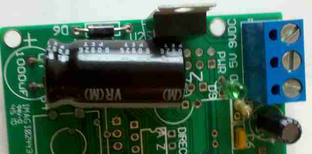
| U2 | LM-7805 or LM-317, TO-220 | 1 | Regulator | |
| R6 | 1K Ohm, 1/8 WATT, | 1 | (For LM-317, not used with LM-7805) | |
| R7 | 330 Ohm, 1/8 WATT, | 1 | (For LM-317, not used with LM-7805) | |
| J4-6 | 3 Pin, 0.2" spacing | 1 | Terminal Block | |
| D6 | 1N4001, 1A, AXIAL | 1 | Reverse protection diode | |
| C4 | 470-1000uF, ELEC, 0.2 RAD | 1 | Main supply filtering (rated above supply voltage) | |
| C5 | 10uF, ELEC, 0.1 RAD | 1 | Main output filtering | |
| C6 | 100nF, CERAMIC, 0.1 RAD | 1 | Secondary output filtering. 22nF supplied. | |
| R5 | 330 Ohm, 1/8 WATT, | 1 | Drives indicator LED | |
| D9 | LED, T1, GRN | 1 | Power indicator light | |
 |
||||
| Q1 | TIP-122, TO-220 | 1 | Darlington Power Transistor | |
| D8 | 1N4001, 1A, AXIAL | 1 | Back EMF protection diode | |
| J7/8 | 2 Pin, 0.2" spacing | 1 | Terminal Block | |
| C8 | ~100nF, CERAMIC, 0.1" RAD | 1 | Ring prevention capacitor | |
| R2 | 2.2 K Ohm, 1/8 WATT | 1 | Signal connection, current limit resistor | |
| D7 | LED, T1, YEL | 1 | Indicator light | |
| R3 | 330 Ohm, 1/8 WATT | 1 | Drives indicator LED | |
  This
cable is pre-wired for the connector
on the Linistepper v2, SLAm and other
PMinMO^ compatible drivers. This
cable is pre-wired for the connector
on the Linistepper v2, SLAm and other
PMinMO^ compatible drivers. |
||||
All the reference designators (e.g. R3, J1, S1) are marked on the PCB as close to pin 1 of that part as is possible.
Square Pad: Pin 1 of a chip or header, or the positive, long, lead on a polarized component always has a square pad.
The assembly documentation is listed here in the order that the kits should be assembled assuming ALL the options are being installed. Skip the sections you don't want, but be sure to assemble in the order presented here: The order of assembly is important as some parts can not be installed after others.
| TOP edge |
 |
| BOTTOM edge |
| TOP edge |
 |
| BOTTOM edge |
When soldering, use a sharp tip and as high a heat as possible. The solder should be standard flux core and as fine as possible. Hold the solder at the point where the lead and the pad on the board meet, then apply the (just cleaned) iron to the other side, again, at the point were the lead and the pad meet. Ensure there is solid contact between the solder and both metal parts, as well as the iron tip and both metal parts. A slight grinding or twisting motion of the iron can be helpful. As soon as the solder melts, or in a few seconds if it doesn't, remove the iron and allow the joint to cool as long as possible. When soldering multi-lead parts like the PIC chip, ribbon cable header or DB25 connector, to avoid heat build up in the plastic case, do NOT proceed in order, but rather always solder what would logically be the coolest lead next. Stubborn points can be eased with a bit of flux dispensed from the point of a pen or pin. See our soldering class for more.
The lowest cost option for connecting the 4Axis board to your PC parallel port is to just take an existing, good quality parallel printer cable and cut off the printer end, then ohm out the wires to find the Data D0-7 signals (pins 2-9 on the PC connector) and strip/solder those wires directly into the holes labeled D0-D7 on the bottom of the 4Axis PCB. Of course, It's a lot quicker to solder on a DB-25 connector and use a parallel extension cable. This connector MUST be a female connector. The cable used from the PC parallel port should be a straight through, male to male as provided in the PC parallel port kit option. The DB 25 connector is pressed onto the edge of the PCB and positioned starting from one corner. Be sure that the pins aline with the pads (it will only align one way) and then work one end on, and slowly rock back and forth to spread the rest of the pins until the PCB edge is fully pressed against the plastic of the connector. Check the pins for alignment to the pads, both top and bottom and re-position as necessary.
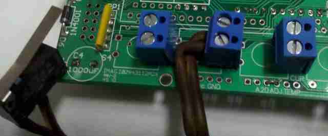
DB 25 connector assembly
The picture below shows the back (bottom) of the PCB, as the DB25 connector is being pushed into place. The row of pins under the solder pads is marked with the signals from the DB25 as they relate to the PC parallel port. The D pins are driven by the PC, and the direction of the other signals is indicated with a little half arrow next to the name.
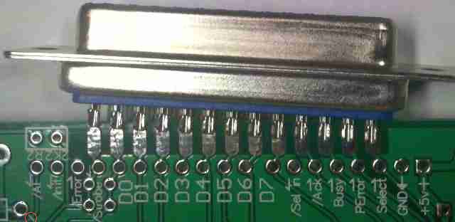
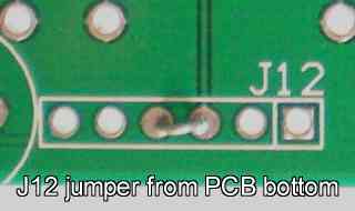
Note: +5 and ground were added and a very slight extra space introduced between D6 and D7 so that the holes could be used with the Arduino controller. This, along with J11 and J12 on the opposite edge of the board, make it an Arduino "Shield".
The next picture, below, is the front of the PCB, and the row of pins under the solder pads is marked with the signals from the DB25 as they relate to how they are used by the drivers and this break out board. Solder each pin, with the iron touching the end of the pin and the pad both at the same time, and the solder fed from the side, near the body of the connector.
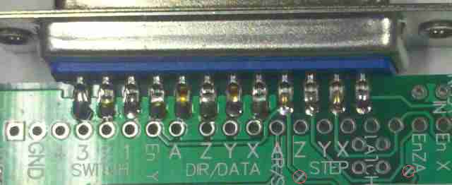
Note: The "En X", "En Y", and "EnZA" each connect to outputs on the PC parallel port so that the drivers can be dropped into low power hold when not in use. It requires a little extra setup in your CNC program, but it's worth it for the temperature control on your motors and drivers. If you really don't want to use those pins, you will need to cut the traces for the enable lines. I've added little circles on these pictures to highlight the marks on the PCB showing good points to cut. There is one in the upper photo in the lower left corner, then two in the lower photo; one under "Z" "STEP", and the other below "EnZA". If you don't configure the lines, make sure your drivers are getting the correct signals. The Linistepper will pull this line low automatically, but the SLAm will put it high (into low power) by default so you will need to ground the enable line on the driver or here on the board.
Signal
PC Port
Pin
XStep D0 2 YStep D1 3 ZStep D2 4 AStep D3 5 XDir D4 6 YDir D5 7 ZDir D6 8 ADir D7 9 Relay nStrobe 1 more below . Also: Setup instructions for Mach3,
Signal PC Port Pin X /EN nAutoFeed 14 Y /EN nSelectIn 17 Z /EN
A /ENnInit 16
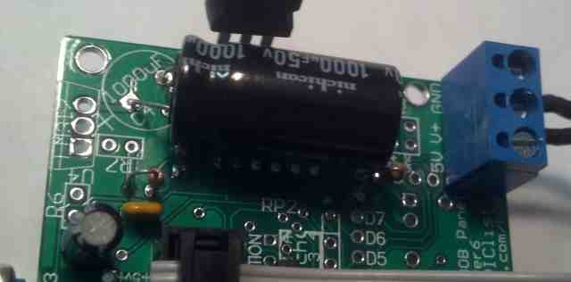
The Power kit provides regulated +5V supply for the divers internal use and for the local options from an unregulated DC power source such as the motor power supply. If your motor supply is more than +12V, or if you are running more than one axis driver, you should probably add a heatsink (it doesn't take a big one) as the regulator may get hot and shut down.You could replace the LM7805 with a switching regulator like the Murata OKI-78SR-5/1.5-W36-C which can take up to 36 volts and still provide 1.5 amps at 5volts.
The version 6 board provides support for the new LM317 kit in place of the 7805. This allows higher motor voltages (up to 50 volts) with a good heatsink or small CPU cooler (heatsink with fan)
Version 5 LM7805 regulator on front
Version 6 LM7805 regulator on front
Version 6 LM317 regulator on back.
Only LED, D6, and terminal on front.Assembly is easy: Most of the components can be mounted from the front or the back of the board. Think about what you want before you start. Mounting on the bottom leaves the front clean for terminal blocks and switches, but requres extra space between the board and the mounting surface.
Mount the diode, D6, first. The end with the band goes in the square hole. Ensure the power regulator, U2 for the LM7805 or U4 for the LM317, is in as shown on the solder mask; with the back to the outside of the PCB when inserted from side where the chip outline is printed. If you run more than one or two axis, you may need a small heatsink. Take care not to cause a short with solder... the holes are very close together.
Be sure to mount the electrolytic capacitors C4-5 with the positive lead in the hole closest to the "+" outside the circle. The positive lead is the one farthest from the stripe on the side of the cap. The big 1000uF cap, C4, can be mounted either on front or underneath.
The long lead of LED D9 needs to be in the square hole toward the resistor R5. The resistor is installed upright; with one lead straight down through one hole and the other bent around and back down through the other hole.
If using the LM317 regulator, install R6 and R7, the 1K and 330 ohm resistors.
Solder the terminal which replaces J4, 5 and 6 on last.
The driver works by grounding the COIL- lead. If you are using a relay with a +5 volt coil, its other lead can be connected to COIL+, which connects to the regulated +5 line. Be sure your +5 supply can handle it. A higher voltage coil can be accomodated by just connecting the other relay lead to an external supply (e.g. +12 or +24 volt) and installing D8 directly across the coil leads. Whatever you do, don't leave D8 out! Reverse EMF protection across the relay coil is critical.Start by installing D8, either on the PCB or directly across the relay coils. The end of the diode without the stripe connects to COIL- in all cases, and the end with the stripe, to the other relay coil lead, usually COIL+.
The TIP122 driver, Q1, can be installed on top or bottom of the PCB, just make sure the pins are in the correct holes. See the part outline in the silkscreen on the bottom.
The LED installs in the little circle just under the Y in RELAY on the front; long lead in the square hole. The other components, R2, R3 and C8 are pretty easy, and can be installed on the back or front. The resistors are standing, with one lead directly in, and the other bent over and looping back down alongside the first.
Leave the terminal blocks for last, and as always, try to work from the center of the board out to the edge.

Before you do this part, make sure you have soldered in the +5 power option and the relay driver as they have components that end up being very close or under JP3.
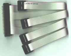
Solder the IDC header JP3 in place on the bottom of the PCB. Pin 1 is clearly marked on the PCB, but harder to find on the header; look for the faint "V" embossed on the side of the header shroud pointing to pin one. The polarity notch should be opposite the DB25 connector. The ribbon cable may not have a polarity nub to match that notch but the red stripe should still be on the pin 1 end and there is another of those very faint "V" symbols embossed above pin one on the connector.
It turns out that not only is it very difficult to see that "V", it's just about impossible to get a picture of it; the "V" is right there, but totally invisible in this picture. At least the picture shows the correct orientation
Note for Arduino users. If you want to mount the BOB to an Arduinio, there really isn't room for this cable on the underside of the BOB. You can mount it on the top, just make sure you also mount the PMIMO connectors on the stepper motor drivers on the bottom of thier PCBs as well. Pin 1 will now be GND, and pin 2 will be X-Enable. Be carefull... check the connectivity before power on.
The other end of of the cable is divided into 4 PMinMO 2x5 connectors
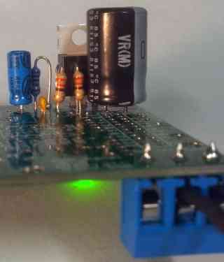
This option drives 3 of the Axis without a PC. It is designed to demonstrate stepper motor control, and test the drivers and motors with a known good signal. Note that this option can NOT be used with the PC option: The board must be build as a PC interface, or a demo/test board, not both. The step and direction signals are developed by a PIC12F675 which is supplied pre-programmed. Because the chip has limited IO, only 3 axis are driven, and the A STEP signal is used as the DIRECTION signal for the other three axis.Because of minor changes between the Version 5 and 6 PCBs, the PIC supplied with this option must be programmed to match the board. If you purchased them together, no worries! If you order this option seperately, please specify the version of the PCB.
Operation: The motors turn one way or the other as you rotate the knob of the pot. As you turn it away from center, nearer either end, the motors will step faster and faster. Turning back from that limit toward the other, the motors will slow, reverse, and then speed up again in the opposite direction. One LED shows the direction of rotation, the other shows the rate of pulses.
Assembly:
Start with two 1K ohm 1/8 watt resistors installed in the last two positions of RP2; between A Step and the A LED, and Z STEP and the Z LED. When you clip off the extra length on the leads, keep them! You will use those to bridge JP4 and JP5, A STEP to all the direction lines, and two pins of J12 (between A2D and ADJ)
Locate J12 on the bottom edge of the front of the board. Bend on of the resistor leads you saved in half and use it to connect pin 3 of J12 ("A2D") to pin 4 ("ADJ") as shown here:
Bend another extra lead length in half and insert it between the holes of JP4, and solder it in place, then clip and discard the remaining length. Repeat for JP5.
You can choose to use or ignore the IC socket. If you use the socket, you can remove the PIC and the A STEP to XYZ DIR jumpers and still connect the board to a PC in the future: Never both install the PIC and jumpers and connect to a PC at the same time! Note that the PIC is installed on the back (bottom) side of PCB. Place and solder the socket or the PIC12F675 pre-programmed chip in the highest position of U1 with the notch on the end toward "U1 PIC". The little dimple on the top of the PIC is nearest pint 1 and should be installed so it is in the square pad, nearest JP5 . Take care to avoid overheating the chip; don't apply heat for more than a few seconds on each lead and solder the leads in a cris-cross pattern, allowing time for each pin to cool before you solder the next closest pin.
Looking at the back of the board, upside down, with the DB 25 pads at the bottom and J11 / J12 at the top, look just to the right of the PIC U1, and find C7 (upside down "C7"). From the round pad of C7 (the one farthest from JP5), move one pad to the right. On the ver6 PCB, this pad is marked as "A3". Jumper that pad to the "S1" pad just below it as shown in the picture.
Install the ~1K ohm (BRN, BLK, RED) resistor between pin 1 and pin 2 of RP1, "S1" to "Vcc" (normally a network resistor, but since we are only using one switch, supplying a single resistor allows us to keep the cost of the kit down), and install the switch in the S1 position.
Install the LED's which will show direction and step signal. When you clip off the extra length on the leads, keep them! You will use those to bridge the X, Y and Z DIRECTION signals to the A STEP signal, as described a little later on.
The LEDs can be installed in two different positions depending on the type of display you like: If the direction LED (installed on the "A" step indicator near the pot) is installed between the square pad (long lead) and the next pad towards the pot, it will light when the motors are going forward, and go out when they turn reverse. In the picture below, the LED on the right is being inserted in that way; long lead in the square hole, short lead pointed to the hole it will fill. If you install it in the pads with the silkscreened circle and the little picture of an LED, it will do the opposite. In either case, the long lead must be in the hole furthest from the pot. The STEP LED is installed on the opposite end of the board, in the "Z" step indicator near U2. If you install it with the long lead in the square hole, the LED will be out most of the time, and flash briefly with each step pulse. If installed in the circle, it will be one most of the time, and blink out briefly with each pulse. In the picture below, the red LED on the left side is being installed in this manner. Again, the long lead must be in the hole farthest "up" the board.
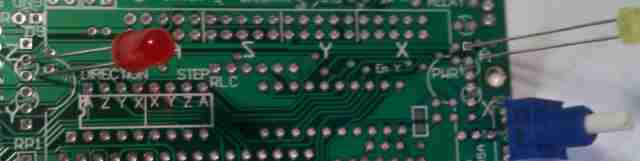
The potentiometer goes on top of the schematic symbol of a variable resistor on the right side of the board, viewed from the front. See the picture above. Because the shaft can be a little hard to turn, we include a "bail lock" which can be screwed onto the shaft for a better grip. Hold the two brackets "spooned" with a clearance hole adjacent a threaded hole and start both screws. Slip the bail lock over the white shaft of the pot and tighten the screws.
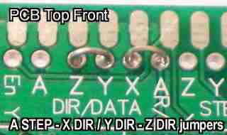
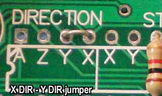
Using the excess leads from the LED's you saved above, jumper the A STEP to X DIR and Y DIR to Z DIR at the top edge of the front of the PCB then jumper X DIR to Y DIR just left of the resistors as shown below. If you would like one motor to always turn forward, you can leave out a jumper. Leave these sticking up a bit so you can clip them if you decide to connect to a PC in the future. Don't connect the board to a PC parallel port while these jumpers are installed, that would short the port pins together and might burn out the port.
Once the pulse parts are installed, you can apply +5 volts via the holes in the upper left corner of the board or by installing the +5 regulator option. The LED's should blink, then begin to operate. When connected to drivers (probably by the Header/4 Axis cable), the motors should begin to turn as you move the pot. When the potentiometer is perfectly centered, it will not pulse at all, so if you don't see a light, turn it left a bit and try again. Right of center, the direction will be low and it will step faster and faster as you reach the limit. Left of center will step in the opposite direction, again, faster as you reach the limit. Pushing the button once should stop the pulsing, then each quick push should step once. Push a bit longer for a burst of pulses and hold the button until the light stays on, then release it to re-start continuous pulsing. Here is a picture of the finished pulse / demo / test unit with the +5 regulator option in operation:
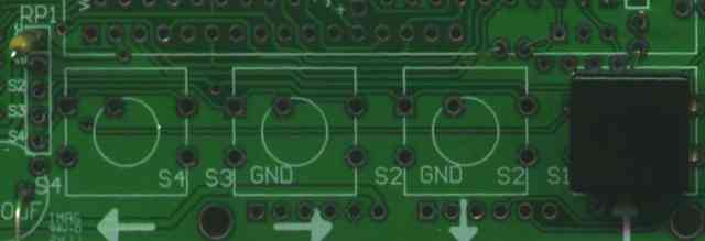
Although a kit is not yet available, you can add limit switches by installing RP1, a 1K to 5K ohm, SIP resistor network (bussed, not isolated) with 5 or more pins. Jameco part 267910 is fine. The pin with the dot goes in the square pad, and if there are more than 5 pin, cut off the extras or just snap the resistor as shown in the picture. The little blue 2 pin headers (Jameco 152347) are optional if you can solder your wire directly into the pads, but they really make it easy for larger wires like the standard ZIP cord used here. Almost any micro switch will work, as long as you can solder your wires to the switch terminals. Here is each switch and the parallel port pin it connects to.
Switch Parallel Port Pin S1 nAck 10 S2 Busy 11 S3 PError 12 S4 Select 13 The switches act by grounding the pin, while RP1 tries to pull the pin up to +5 volts. The direct connection of the switch can always overpower the resistor, so the result is ground when the switch contacts meet and +5 when they are open.
For the Version 6 and later PCB, the mounting holes are located as follows:
| # | X | , Y |
|---|---|---|
| 1. | 0.90" | , 0.49" |
| 2. | 0.11" | , 2.15" |
| 3. | 1.19" | , .011" |
| 4. | 3.20" | , 0.11" |
| 5. | 3.57" | , 1.14" |
None at this time.
| Video instructions for building the most common options of the BOB Panel board. |
Douglas Cook Says:
DB-25 PC Parallel Port kit: Should have a option for just the Connector as some people may require the Connector but don't want to add the Printer cable because they have a standard Printer/Parallel cable.+
Questions:
Comments:
See also:
| file: /Techref/io/stepper/linistep/4axis5build.htm, 38KB, , updated: 2020/7/7 11:13, local time: 2025/10/21 09:23,
216.73.216.53,10-2-207-162:LOG IN
|
| ©2025 These pages are served without commercial sponsorship. (No popup ads, etc...).Bandwidth abuse increases hosting cost forcing sponsorship or shutdown. This server aggressively defends against automated copying for any reason including offline viewing, duplication, etc... Please respect this requirement and DO NOT RIP THIS SITE. Questions? <A HREF="http://massmind.org/techref/io/stepper/linistep/4axis5build.htm"> Break Out Board, Logic Power Regulator, Relay Driver, Indicators, Switches, Microchip PIC, LCD Panel, Current and Temp sensors.</A> |
| Did you find what you needed? |
Welcome to massmind.org! |
|
Ashley Roll has put together a really nice little unit here. Leave off the MAX232 and keep these handy for the few times you need true RS232! |
.